Heat Treatment Equipment for Advanced Semiconductor Packaging
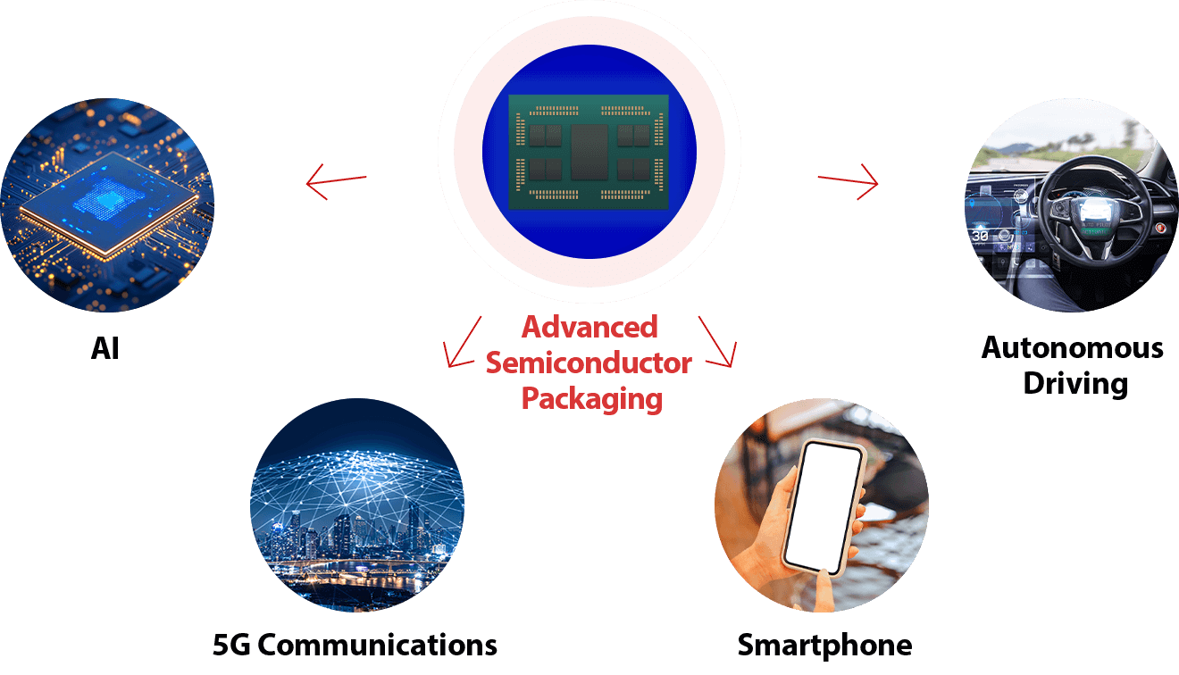
Demand for high-performance semiconductors is rapidly increasing due to the spread of IoT, 5G, AI, etc. High integration through miniaturization is approaching its limits in terms of technology and cost, and advanced semiconductor packaging technologies such as 2.5D and 3D are attracting attention. JTEKT Thermo Systems provides various heat treatment equipment for advanced semiconductor packaging, and contribute to the manufacturing of next-generation semiconductors.
What is Advanced Semiconductor Packaging?
Advanced semiconductor packaging is a semiconductor product that contains multiple semiconductor chips with different functions in a single package, with multiple chips (chiplets) densely mounted. They are called 2.5D-IC or 3D-IC. The distance between chips on them is shorter than those in which each chip is mounted in a separate package, resulting in faster information transmission. In addition, combining chips with different functions reduces costs, improves yields, and increases productivity, rather than manufacturing a single large chip with multiple functions.
Traditionally, the semiconductor manufacturing process has been a division of labor, with foundries in charge of front-end processes and OSAT companies in charge of back-end processes. However, in the manufacturing of advanced semiconductor packages, both front-end and back-end process technologies can be utilized, and thus, companies in both fields are entering the market.
Advanced semiconductor packaging technologies with high performance are used in various fields and products such as AI, high-performance computing, 5G communications, smartphones, IoT devices, and autonomous driving.
Heat Treatment Process for Advanced Semiconductor Packaging
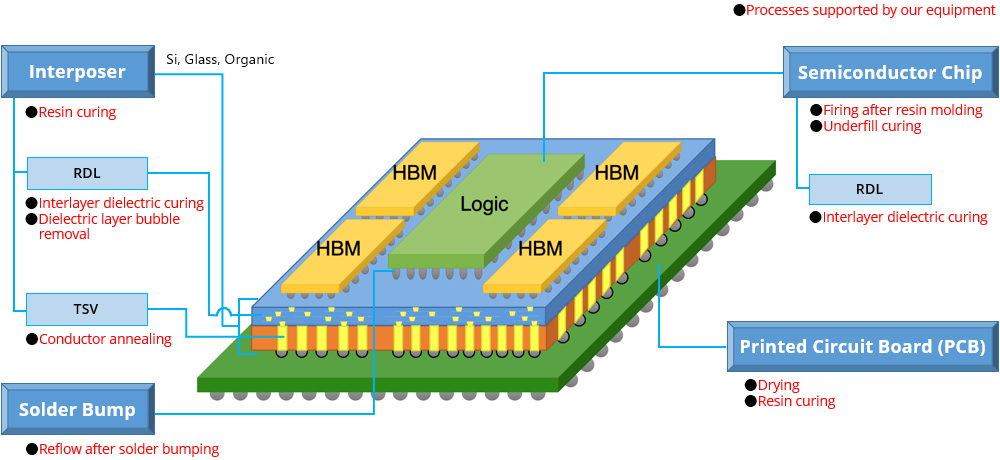
Our furnaces and ovens are available for the drying of printed circuit board (PCB), various heat treatments for Si interposer, RDL (Redistribution Layer), glass interposer, etc., reflow after solder bumping, and baking after chip molding. We also have extensive experience in supplying heat treatment equipment for FO-WLP (Fan Out-Wafer Level Package) and WL-CSP (Wafer Level-Chip Size Package).
Leveraging our experience and technology accumulated through the manufacturing equipment for semiconductor and LCD substrate, we provide equipment for various manufacturing processes of advanced semiconductor packages.
Product Lineup
-
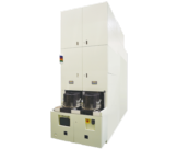
Clean oven
SO2-12-F -
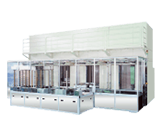
Vertical Furnace
VF-5700B-F2 -
Vertical Furnace
VF-5900B -
Large Bore Vertical furnace
VFS-4000 -
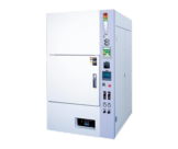
Clean Oven
CLH-21CD
| Model | Mass-Production | R&D | |||
|---|---|---|---|---|---|
| Clean Oven | Vertical Furnace | Large Bore Vertical Furnace | Clean Oven | ||
| SO2-12-F / SO2-30-F SO2-12L-F / SO2-30L-F |
SO2-60-F | VF-5700B-F2 VF-5900B |
VFS-4000 | CLH-21CD(H) CLH-35CD(H) |
|
| FO-WLP | 〇 | ― | 〇 | ― | 〇 |
| FO-PLP | 〇 | 〇 | ― | 〇 | 〇 |
| Si Interposer | 〇 | ― | 〇 | ― | 〇 |
| Glass Interposer | 〇 Support square/ round wafer |
〇 Support square/ round wafer |
〇 Support only round wafer |
〇 Support square/ round wafer |
〇 Support square/ round wafer |
| Organic Interposer | 〇 Support square/ round wafer |
〇 Support square/ round wafer |
〇 Support only round wafer |
〇 Support square/ round wafer |
〇 Support square/ round wafer |
| Wafer size (mm) | Φ300 300×300 |
510×515 600×600 |
Φ300 | 300×300 510×515 600×600 |
Φ300 300×300 |
| Chamber | 2 | 2 | 1 | 1 | 1 |
| Max. process volume*1/ Chamber |
50 pcs.*2, 52 pcs.*3 |
24 pcs. | 75 pcs.*4, 100 pcs.*5 |
12 pcs. | ― |
| Heating method | Hot air circulating type | Electric resistance heating type | Hot air circulating type | ||
| Wafer transfer | Transfer robot | Manual | |||
| I/O port (FOUP) | 4 | 4 | 2 | 2 | ― |
| Temp. range | 70~450℃*2, 70~400℃*3 |
70~300℃ | ~750℃ | ~600℃ | RT+70~530℃ |
| Residual O2 density | <10ppm | <20ppm | |||
| Self cleaning | ― | ― | Burn out | ― | |
*1 It may vary depending on wafer thickness and warpage.
*2 The figures for SO2-12-F / SO2-30-F
*3 The figures for SO2-12L-F / SO2-30L-F
*4 The figures for VF-5700B-F2
*5 The figures for VF-5900B